
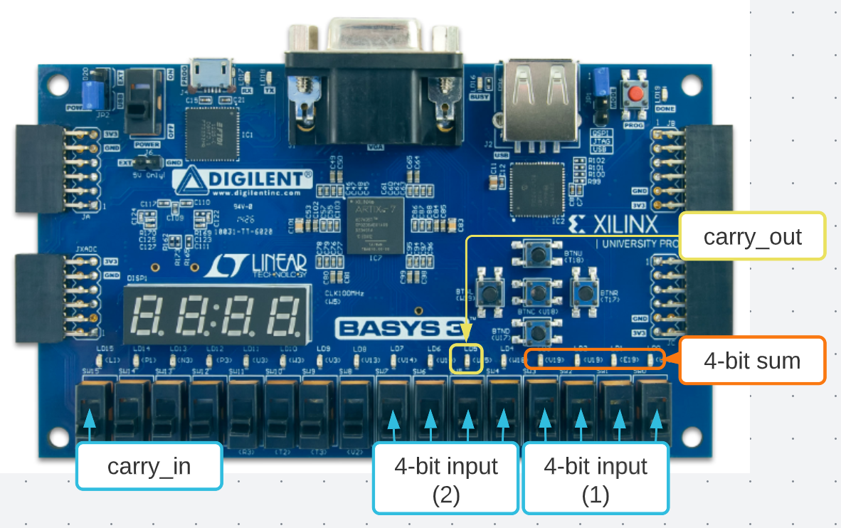
Implementation of full adder circuit in Verilog for the Basys3 board using the free version of the Vivado 2022.1 IDE. The hardware implementation of the full adder adds two 4-bit binary numbers and displays the answer using the LEDs.
Basys3 Atix-7 FPGA
The Basys 3 is an entry-level FPGA development board. It includes the standard features for Basys boards, such as:
- complete ready-to-use hardware
- a large collection of on-board I/O devices
- all required FPGA support circuits
- a free version of development tools
Specifications
- 4 Pmod ports: 3 Standard 12-pin Pmod ports, 1 dual purpose XADC signal / standard Pmod port
- 4-digit 7-segment display
- 5 user pushbuttons
- 16 user LEDs
- 16 user switches
- USB HID Host for mice, keyboards and memory sticks
- 12-bit VGA output
- USB-UART Bridge
- Serial Flash
- Digilent USB-JTAG port for FPGA programming and communication
- On-chip analog-to-digital converter (XADC)
- Internal clock speeds exceeding 450 MHz
- 90 DSP slices
- Five clock management tiles, each with a phase-locked loop (PLL)
- 1,800 Kbits of fast block RAM
- 33,280 logic cells in 5200 slices (each slice contains four 6-input LUTs and 8 flip-flops)
- Features the Xilinx Artix-7 FPGA: XC7A35T-1CPG236C
Overall, a very nice, beginner friendly board. With many inputs / outputs ready available without expansions, it is truly a great starting /advanced hardware.
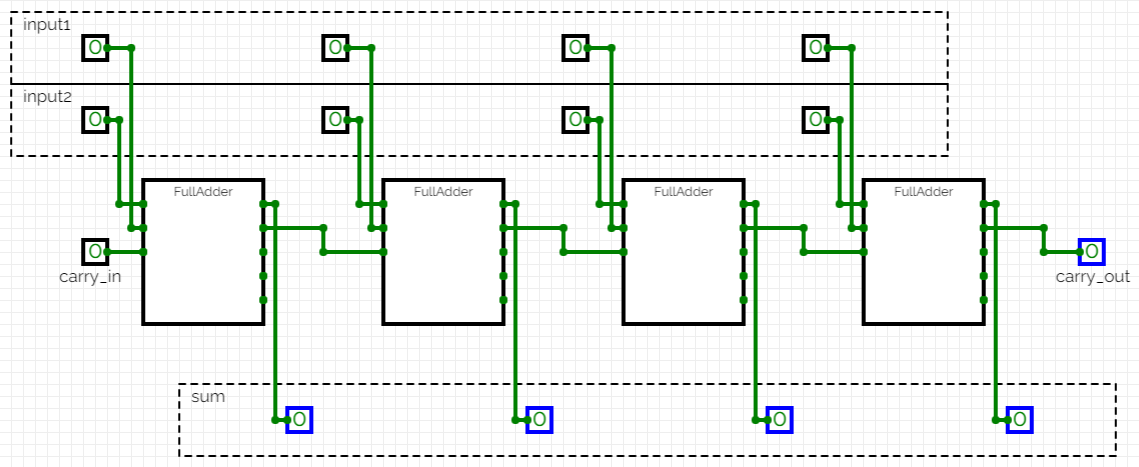
Diagram
Here is a diagram of full adder logic. It can be studies in more details in the previous post on how to implement it in Python.

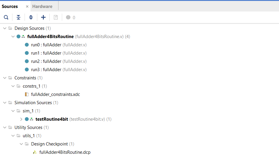
Sources Overview
Below is the overview of all the sources needed to complete the task on FGPA Basys3 board.
Design Sources
fullAdder.v
Full adder code, constructed from two half adders, as on above diagram.
// Full adder routine


`timescale 1ns / 1ps

module fullAdder(
    sum,
    carry_out,
    input1,
    input2,
    carry_in
    );

    output sum, carry_out;
    input input1, input2, carry_in;

    wire sum1, connection1, connection2;

    xor (sum1, input1, input2);
    and (connection1, input1, input2);
    xor (sum, sum1, carry_in);
    and (connection2, sum1, carry_in);
    or (carry_out, connection2, connection1);

endmodule
fullAdder4BitsRoutine.v
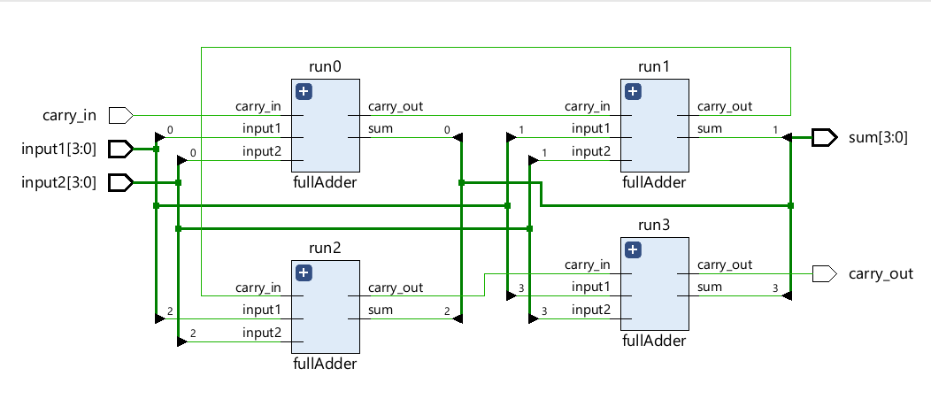
Main full adder module that calls the above sub-module 4 times. To illustrate the operation, study the diagram below:
// Full adder circuit on 4-bits using full adder routine constructed from two halfs

`timescale 1ns / 1ps

module fullAdder4BitsRoutine(
    sum,
    carry_out,
    input1,
    input2,
    carry_in
    );

    output [3:0] sum;
    output carry_out;
    input [3:0] input1, input2;
    input carry_in;

    wire connection1, connection2, connection3;
    fullAdder run0(sum[0], connection1, input1[0], input2[0], carry_in);
    fullAdder run1(sum[1], connection2, input1[1], input2[1], connection1);
    fullAdder run2(sum[2], connection3, input1[2], input2[2], connection2);
    fullAdder run3(sum[3], carry_out, input1[3], input2[3], connection3);

endmodule
Constraints
Setup the IO on the FPGA board. I have used the default Basys3 constraints file and modified to suit. Diagram below shows what is used.
fullAdder_constraints.xdc
## Switches - first 4bit input
set_property PACKAGE_PIN V17 [get_ports {input1[0]}]
set_property IOSTANDARD LVCMOS33 [get_ports {input1[0]}]
set_property PACKAGE_PIN V16 [get_ports {input1[1]}]
set_property IOSTANDARD LVCMOS33 [get_ports {input1[1]}]
set_property PACKAGE_PIN W16 [get_ports {input1[2]}]
set_property IOSTANDARD LVCMOS33 [get_ports {input1[2]}]
set_property PACKAGE_PIN W17 [get_ports {input1[3]}]
set_property IOSTANDARD LVCMOS33 [get_ports {input1[3]}]

## Switches - second 4bit input
set_property PACKAGE_PIN W15 [get_ports {input2[0]}]
set_property IOSTANDARD LVCMOS33 [get_ports {input2[0]}]
set_property PACKAGE_PIN V15 [get_ports {input2[1]}]
set_property IOSTANDARD LVCMOS33 [get_ports {input2[1]}]
set_property PACKAGE_PIN W14 [get_ports {input2[2]}]
set_property IOSTANDARD LVCMOS33 [get_ports {input2[2]}]
set_property PACKAGE_PIN W13 [get_ports {input2[3]}]
set_property IOSTANDARD LVCMOS33 [get_ports {input2[3]}]

## Switches - carry_in bit
set_property PACKAGE_PIN R2 [get_ports {carry_in}]
set_property IOSTANDARD LVCMOS33 [get_ports {carry_in}]

## LEDs
set_property PACKAGE_PIN U16 [get_ports {sum[0]}]
set_property IOSTANDARD LVCMOS33 [get_ports {sum[0]}]
set_property PACKAGE_PIN E19 [get_ports {sum[1]}]
set_property IOSTANDARD LVCMOS33 [get_ports {sum[1]}]
set_property PACKAGE_PIN U19 [get_ports {sum[2]}]
set_property IOSTANDARD LVCMOS33 [get_ports {sum[2]}]
set_property PACKAGE_PIN V19 [get_ports {sum[3]}]
set_property IOSTANDARD LVCMOS33 [get_ports {sum[3]}]
set_property PACKAGE_PIN U15 [get_ports {carry_out}]
set_property IOSTANDARD LVCMOS33 [get_ports {carry_out}]
Simulation Sources
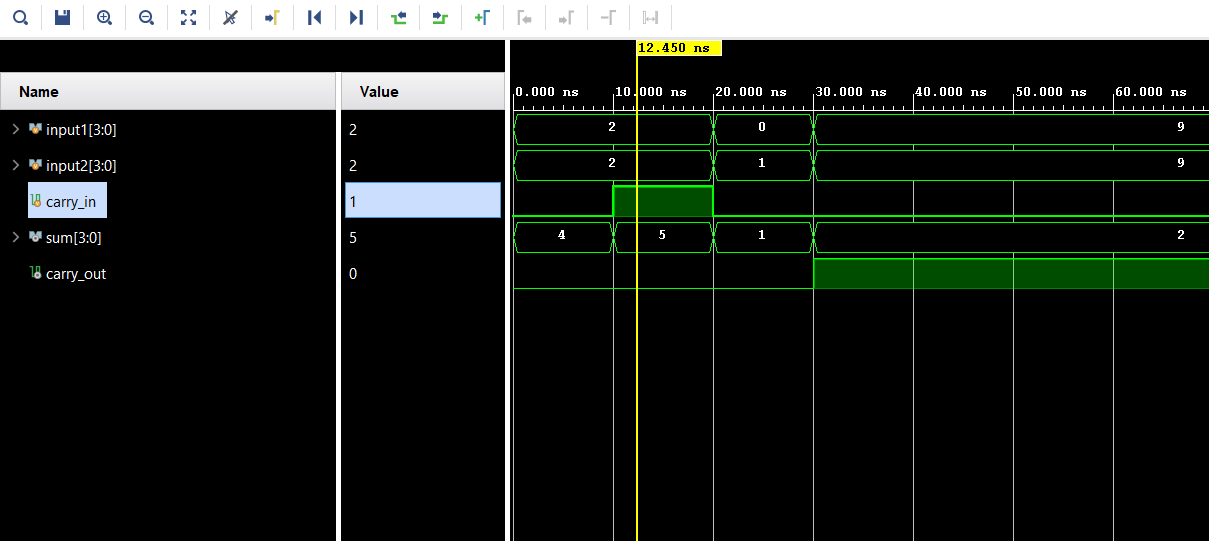
Additionally, we can create a simulation file, to run the behawior simulation of the hardware implementation. This is preferable, but optional file that is not required to be uploaded to the FPGA.
testRoutine4bit.v
// Testing the implementation with 4bit inputs

`timescale 1ns / 1ps

module testRoutine4bit;
reg [3:0] input1, input2;
reg carry_in;
wire [3:0] sum;
wire carry_out;

fullAdder4BitsRoutine testRun (sum,carry_out,input1,input2,carry_in);

initial
begin

$monitor ($time, "INPUT1 = %b, INPUT2 = %b, CARRY_IN = %b, CARRY_OUT = %b, SUM = %b\n",input1, input2, carry_in, carry_out, sum);

end
initial
begin

// inputs as 4-bit, carry_in as binary 0 or 1
input1 = 4'b0010; input2 = 4'b0010; carry_in = 1'b0;
#10
input1 = 4'b0010; input2 = 4'b0010; carry_in = 1'b1;
#10
input1 = 4'b0000; input2 = 4'b0001; carry_in = 1'b0;
#10
input1 = 4'b1001; input2 = 4'b1001; carry_in = 1'b0;

end

endmodule
The results are used to confirm correct operation by studying the signal change.
RTL Analysis
We can view the schematic by going to RTL Analysis – > Schematic menu. The above code has 4 runs of fullAdder.v and generates sum[3:0] and carry_out bits.
Generating Bitstream
After running the Synthesis and Simulation, the bitstream needs to be generated. I have used additional option to generate .bin file, so I can upload it to the on-board memory. This will enable me to run the program after power cycle.
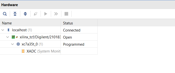
First, detect and connect to the hardware.
Programming Flash Memory
By default, the generated bitstream is sent to the FPGA Basys3 board via the USB cable. It is saved to the (volatile) SRAM-based memory cells within the FPGA, but only stay there until power cycle / reset.
However, we are able to program pn-board non-volatile SPI Flash memory, so the program is persistent after power cycle. It is simply reloaded to the volatile memory from the flash upon reboot.
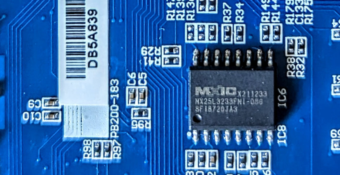
Memory Type
It is important that you note your memory type of your Basys3 board as they differ, depends on the year of manufacture. Below is example of what I found on my board:
To configure the memory, go to Add Configuration Memory Device and set your memory type there. For this reason, the .bin file generated above is used to program the non-volatile memory.
Demonstration
I have taken photographs to illustrate a few possible 4-bit input configurations and the results.
0001 + 0001 = 0010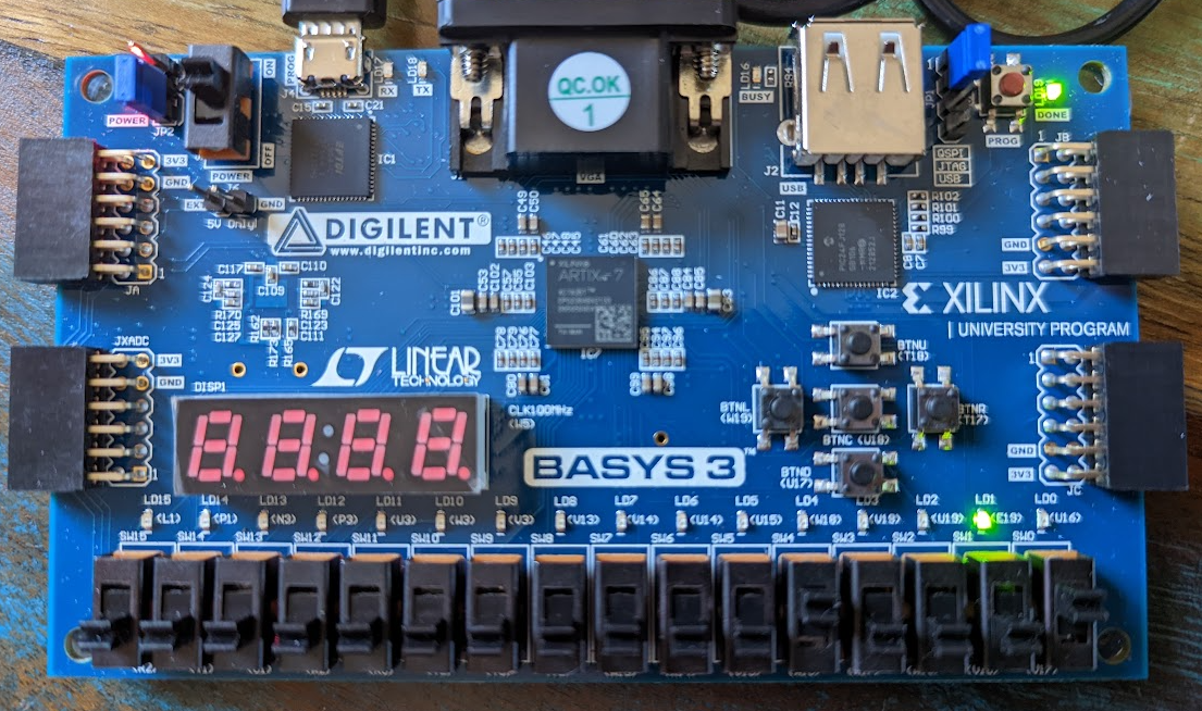
0011 + 0011 = 0110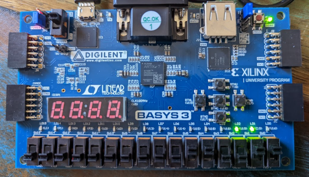
1000 + 1000 = (1)0000 = (carry_out bit) + 0000